
Introduction: Exploding Information Volume and the “Electricity Wall
Our society is now overflowing with an unprecedented amount of information due to the evolution of generative AI, the growth of huge data centers, and the proliferation of IoT devices. The “wiring” that connects the inside of semiconductor chips (LSIs) and between servers supports this digital society from the ground up. However, the “electrical wiring” conventionally used is approaching its physical limits in terms of performance improvement.
Signal delays, increased power consumption, and heat generation–these problems are known as “electrical barriers” and are major obstacles to further performance improvements. These problems, also known as the “electrical wall,” are major obstacles to further performance improvement. The technology that is currently attracting the most attention from researchers and companies around the world as the key to breaking through this barrier is “optoelectronic fusion.
Optoelectronic fusion is a technology that combines the advanced computing and control capabilities of electronic circuits with the advantages of high-speed, large capacity, and low power consumption of optical communications on a single chip. However, simply combining electricity and light is not enough. To realize its true value, it was necessary to “densely integrate” optical circuits to the same level as electronic circuits.
This article will take an in-depth look at why high integration of photoelectric fusion was necessary, what technological breakthroughs made it possible, and the physical limitations that still exist and the cutting-edge challenges to overcome them.
Chapter 1: Why did it have to be light? -The Limitations of Electrical Wiring and the Expectations of Light
Computer performance has evolved tremendously by increasing the number of transistors in integrated circuits, in accordance with “Moore’s Law. However, as chips became more powerful and larger, the length of the internal electrical wiring continued to increase, which began to create a serious bottleneck.
The longer the electrical signals are routed and the higher the signal frequency, the greater the signal degradation and delay. In addition, the heat generated by electrical resistance interferes with the stable operation of the chip and consumes enormous amounts of power for cooling. This electrical wiring problem is a major reason why power consumption in data centers has become a global issue.
This is where “light ” came in. As fiber-optic communications have proven, light is overwhelmingly faster than electrical signals, and its signals are less susceptible to degradation even when transmitted over long distances, and its power consumption is an order of magnitude lower.
If we can replace electricity with light inside LSI chips and for communication between chips, we may be able to solve at once the wiring problem that has been a stumbling block to performance improvement. This is the basic idea behind “optoelectronic fusion.
However, achieving this goal is not easy. The most important and difficult challenge for this technology is the “high integration” of electronic circuits and optical devices, which have evolved in separate worlds, onto a chip a few centimeters square and with a density comparable to that of electronic circuits.
Chapter 2: Revolution in the Micro World! Two Innovations Enabling High Integration
In order to make optical circuits as small as electronic circuits, it was necessary to overcome the physical properties of light itself, particularly the limitation of “wavelength. Because of the wave nature of light, it has been extremely difficult to reduce the width of the “optical waveguide,” which is the pathway for light, to less than the wavelength of light (approximately 1.55 μm = 1550 nm used in communications). However, two innovative technologies are turning this conventional wisdom on its head.
Innovation 1: Silicon Photonics
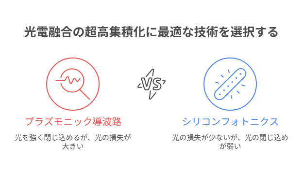
The first is “silicon photonics. This is a technology for creating optical circuits using silicon, which has long been used in the semiconductor industry. Silicon is characterized by the extremely large difference in refractive index between the “core,” which allows light to pass through, and the “cladding” (quartz, etc.) that covers it. This large refractive index difference makes it possible to strongly confine light and reduce the width of an optical waveguide to a few hundred nanometers (nm), which is much smaller than the wavelength. Another major advantage of this technology is that it can be manufactured at low cost and with high precision because existing semiconductor manufacturing processes can be applied.
Innovation 2: Plasmonic Waveguides
The second is “plasmonic waveguide,” which goes even further. This technology utilizes the collective oscillation of special electrons called “surface plasmon polaritons” that occur at the boundary between a metal and a dielectric (a material that does not conduct electricity). Using this phenomenon, it is possible to confine the energy of light to an extremely small area of several tens of nanometers, far beyond the wavelength limit. This is no longer at the same level as the wiring width of an electronic circuit, and is a game changer that paves the way for ultra-high integration of photoelectric fusion.
However, plasmonic waveguides are a double-edged sword, as the price to pay for the strong confinement of light is the large loss of light during transmission.
These innovations have dramatically miniaturized optical circuits, making high-density integration with electronic circuits a reality.
Chapter 3: The Physical Wall that Stands in the Way – The Dilemma of “Turning the Corner
Although technological advances have reduced the width of optical waveguides to an absolute minimum, a new physical barrier still stands in the way of higher integration. This is the “radius of curvature limitation,” or “bend angle” problem.
Just as forcibly bending a fiber-optic cable will result in loss of communication, if a microscopic optical waveguide on a chip is bent in a sharp curve, light will leak out, resulting in signal degradation known as “bending loss. Therefore, when bending a waveguide, the curve must be gentler than the “minimum radius of curvature” at which the loss falls within an acceptable range.
Even if the width of the waveguide is a few hundred nm, if the radius of curvature is several millimeters, it will occupy a large area when routing the wiring on the chip, which is a major obstacle to high integration.
Using silicon photonics, this minimum radius of curvature can be reduced to a few micrometers (μm), but there is still a limit. Furthermore, even plasmonic waveguides, the ultimate miniaturization technology, cannot completely escape this bending loss, and the minimum radius of curvature is limited to about 8 to 10 μm.
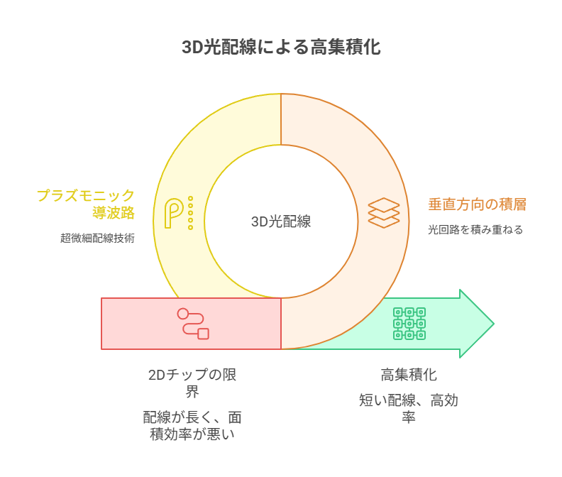
This “bend” dilemma suggested that the conventional idea of cramming circuits onto a flat (2D) surface itself had its limitations.
Chapter 4: Beyond Dimensions! The Final Answer: “3D Optical Wiring
When the physical limits of flat-panel integration were reached, engineers turned their thinking around. If we can’t lay them out horizontally, why not stack them vertically? This was the final answer: “3D (three-dimensional) optical wiring,” which is now at the forefront of optoelectronic integration technology.
When wiring is routed on a 2D chip, it inevitably takes a long way around or crosses in complex ways, consuming a lot of area. However, if a 3D structure is used, in which layers of optical circuits are stacked above and below the electronic circuit LSI, signals can be exchanged over the shortest possible distance. This not only dramatically shortens wiring lengths, reducing delays and power consumption, but also dramatically improves the area efficiency of the entire chip.
In Japan, the national project PETRA and others have succeeded in demonstrating the world’s first 3D optical wiring technology that integrates LSI chips and optical ICs in a single layer. This is an epoch-making approach that solves the limitation of chip area in a new dimension of “volume.
Ultra-fine wiring technologies such as plasmonic waveguides are also very compatible with this 3D technology, and in the future, by creating light pathways in the vertical direction as well, a three-dimensional, ultra-dense optical network will be constructed inside the chip, just like buildings in a city.
The 2D limitation of “turning the corner” is overcome by 3D integration. This is the current mainstream strategy to bring the high integration of photoelectric fusion to the next level.
Summary: The Power of Light to Pioneer the Digital Society of the Future
This article traces how “optoelectronic fusion,” which emerged to overcome the limitations of electrical wiring, has achieved high integration.
- The innovations of silicon photonics andplasmonic waveguides have paved the way for miniaturization of optical circuits to the level of electronic circuits.
- However, the physical limitation of “radius of curvature” became a new barrier to high integration on a flat surface.
- To break through this barrier, “3D optical wiring” technology is currently being used to achieve higher integration beyond dimensions.
Photoelectric fusion technology is no longer a laboratory-level story. Its implementation is steadily advancing as an indispensable fundamental technology that will support the explosive evolution of next-generation data centers, supercomputers, and AI. Behind the scenes of the digital society we take for granted, a quiet revolution is now underway to overcome the limitations of electricity with light.